Hey there! As a pogo PCB supplier, I've seen firsthand how a well - optimized layout can make all the difference in the performance and functionality of a pogo PCB. In this blog, I'm gonna share some tips and tricks on how to optimize that layout.
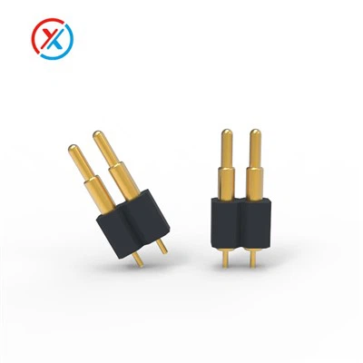
First off, let's talk about what pogo PCBs are. Pogo PCBs use pogo pins, which are spring - loaded pins. They're super useful in making temporary electrical connections, and you can find them in all sorts of electronic devices. You can check out more details about these pins on our Pogo Pin Supplier page.
Understanding the Basics of Pogo PCB Layout
Before we start optimizing, we need to understand the basics. The pogo pins on a PCB are like little bridges, creating connections between different parts of a circuit. It's crucial to know the spacing requirements between these pins. If the pins are too close, there could be short - circuits or interference. On the other hand, if they're too far apart, it can take up unnecessary space on the PCB.
The Spring Contact Pins have different sizes and shapes. You need to choose the right ones for your specific project. Smaller pins might be more suitable for dense circuits, while larger ones could handle more current.
Pin Placement
One of the most important steps in optimizing the layout is pin placement. You should group the pins based on their functions. For example, all the power pins should be placed close to each other, and the same goes for signal - carrying pins. This helps in reducing electromagnetic interference (EMI). EMI can cause all sorts of problems, like signal distortion or even system failures.
When placing the pins, also think about the ease of connection. If the PCB is going to be used in a device where it needs to be frequently connected and disconnected, make sure the pin arrangement is accessible. You don't want users struggling to align the pogo pins properly.
Layer Utilization
Most PCBs have multiple layers, and you need to use them wisely. For pogo PCBs, you can separate different types of signals on different layers. For instance, you can put the high - speed signals on one layer and the power lines on another. This separation helps in further reducing interference.
The Spring Pogo Pin connections should be routed in a way that they don't cross over each other on different layers. This can cause signal degradation and other issues. When routing the traces for the pins, try to keep them as short as possible. Shorter traces mean less resistance and better signal quality.
Thermal Management
Pogo PCBs can generate heat, especially if they're carrying high currents. That's why thermal management is a big deal. You can add thermal vias near the power - carrying pins. These vias act as heat sinks, dissipating the heat away from the pins and the PCB.
Also, make sure there's enough space around the pins for proper air circulation. If the pins are packed too tightly, the heat won't be able to escape, which can lead to overheating and damage to the pins and the PCB.
Design for Manufacturability
When you're designing the pogo PCB layout, it's important to think about the manufacturing process. Make sure the pin holes and pads are of the right size and shape for the manufacturing equipment. The Surface Mount Pogo Pins require a different design approach compared to through - hole pins.
You should also consider the tolerances of the manufacturing process. If you specify very tight tolerances, it might make the manufacturing process more difficult and expensive. Strike a balance between the required precision and what's practically achievable.
Testing and Validation
Once you've designed the layout, it's time to test it. You can use simulation software to test how the pogo pins will perform under different conditions. This can help you identify any potential issues before you start mass - producing the PCBs.
You can also create a prototype. A prototype allows you to physically test the pogo PCB and make any necessary adjustments. You might find that some pin placements need to be changed or that the thermal management isn't working as expected.
Material Selection
The choice of materials for your pogo PCB is crucial. The substrate material should have good electrical and thermal properties. For the pogo pins themselves, you should consider factors like conductivity, durability, and corrosion resistance. The Lead - Free - Pogo - Pins High Quality are a great option for those looking for environmentally friendly and high - performing pins.


The plating on the pins also matters. A good plating can reduce contact resistance and improve the overall performance of the pogo pins.
Cost - Effectiveness
While optimizing the layout, you also need to keep an eye on the cost. Using high - end materials for every part of the PCB might not be necessary. You can look for cost - effective alternatives that still meet your performance requirements.
For example, instead of using the most expensive substrate material, you can find a more budget - friendly option that still provides adequate electrical and thermal properties. And when it comes to the pogo pins, choose the ones that offer the best balance between cost and performance.
Future - Proofing
As technology keeps evolving, your pogo PCB should be able to adapt. You can design the layout in a way that allows for future upgrades. For example, leave some extra space on the PCB for additional components or features.
Also, keep an eye on industry trends. New types of pogo pins or PCB manufacturing techniques might become available in the future. Make sure your design can incorporate these advancements without having to do a complete overhaul.
Wrapping Up
Optimizing the layout of a pogo PCB is a complex but rewarding process. By following these tips on pin placement, layer utilization, thermal management, and more, you can create a high - performing, cost - effective, and future - proof pogo PCB.
If you're interested in purchasing high - quality pogo PCBs or have any questions about the optimization process, don't hesitate to reach out. We're here to help you with all your pogo PCB needs. Whether you're working on a small project or a large - scale production, we have the expertise and the products to support you.
References
- Electronics Design Handbook
- PCB Manufacturing Best Practices Guides
- Industry whitepapers on pogo pins and PCB design