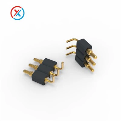
Hey there, if you’ve ever worked with electronics—whether you’re a design engineer, a procurement lead, or just someone who geeks out over how your phone’s charger connects or a drone’s circuit boards talk to each other—you’ve probably crossed paths with pogo PCBs. Wait, let’s back up: pogo PCBs aren’t just regular circuit boards, right? They’re paired with pogo pins (the tiny, spring-loaded little guys that make the physical connection between two parts) to do signal transmission. Today, I want to break down exactly how their signal transmission performs, because as a pogo pin supplier who’s been in this game for years, I’ve seen firsthand how the right pogo PCB setup makes or breaks a device’s reliability.


First, let’s get the basics straight: signal transmission performance here basically boils down to three things—signal loss, impedance consistency, and crosstalk. For context, when a signal travels through a wire or a connector, some of it fizzles out (that’s loss), if it bounces back because the connection’s not uniform that messes things up (impedance mismatch), and if signals from nearby lines bleed into each other (crosstalk), that causes errors. Pogo PCBs, since they use those spring-loaded pogo pins to create the connection between the PCB’s two layers (like the main board and a sub-board, or a test fixture and a product), have to nail all three to work well.
Let’s start with signal loss, because that’s the biggest pain point most people complain about. What causes loss with pogo PCBs? Two main culprits: resistance in the pogo pins themselves, and gaps at the connection point. Pogo pins are usually made of copper alloys (like brass or beryllium copper) with a gold plating for corrosion resistance and conductivity. But gold’s thin—usually around 5-10 micro inches, depending on the application—and if you go too cheap on plating, or if the pogo pins aren’t aligned right when pressed into the PCB, you get tiny gaps between the pin and the PCB’s contact pad. Those gaps add contact resistance, which eats into your signal. As a pogo pin supplier, I’ve worked with engineers who tried to use off-brand pogo pins with rough plating, and their signal loss was 2-3x higher than expected—enough to make a high-speed sensor fail.
Wait, but it’s not just the pin. The PCB side matters too. Pogo PCBs for high-frequency apps (like 5G devices or high-speed data test fixtures) use trace widths and spacing tuned for a specific impedance, usually 50 ohms for single-ended signals or 100 ohms for differential pairs. If the PCB’s contact pads for the pogo pins aren’t sized to match the pin’s diameter (we have 1mm pogo contacts that work perfectly with standard 1mm traces), you get a sudden impedance change at the connection point. That impedance mismatch causes reflection, which is a type of signal loss called return loss. For high-speed signals (above 1 Gbps), even a 0.1mm mismatch can add 1-2 dB of loss per connection. Multiply that over a few connections, and you’re looking at a signal that’s too weak to read at the other end.
Then there’s crosstalk, which is the uninvited guest at the signal party. Pogo PCBs have a bunch of pogo pins lined up next to each other, right? So if two pins carry high-speed signals running parallel, the electromagnetic field from one can leak into the other. That’s crosstalk, and it’s worse when the pins are too close together or the PCB’s ground planes aren’t placed right. Here’s where pogo pin design comes in: if the pins have a non-conductive coating on the sides between the signal contacts, that cuts down on that leakage. Also, the PCB’s ground traces between signal traces act like a barrier, so a well-designed pogo PCB will have a ground plane that’s connected to every other pogo pin’s ground point, not just spaced out. I’ve seen test fixtures with bad pogo PCB design that had crosstalk levels of -20 dB, which is way too high for 10 Gbps Ethernet—you start seeing bit errors every few minutes. Fix that by spacing pins 2x their diameter and adding ground planes, and crosstalk drops to -35 dB, which is totally acceptable.
Now, let’s talk about real-world use cases to make this concrete. Take consumer electronics: when you plug in a wireless earbud case for charging, the pogo pins on the case’s PCB have to transmit both power and data (to check battery levels) without losing too much. If the signal loss was too high, the earbud case would incorrectly show full battery when it’s actually low. Another example: industrial test fixtures for circuit boards. These fixtures use pogo PCBs to connect to the board’s test points, often running signals at 5 Gbps for high-speed data transfer during testing. Here, consistent impedance is non-negotiable—if every pogo pin’s connection has a slightly different impedance, the test data gets garbled, leading to false failures. And that’s where working with a reputable pogo pin supplier (check out our pogo pin supplier page for details) makes a huge difference, because we engineer pins with tight dimensional tolerances so they seat flush with the PCB’s pads every single time.
Wait, let’s address a common myth: people think pogo PCBs only work for low-speed signals, but that’s not true. I’ve seen pogo PCBs handle up to 20 Gbps differential signals when the design is right. The key is matching the pogo pin’s characteristics to the PCB’s. For example, lead-free pogo pins (another one of our lines, you can see them here) have a slightly different plating thickness than tin-plated ones, so you have to adjust the PCB’s pad size to keep impedance consistent. We’ve done custom setups for 10 Gbps camera modules where the pogo PCB was the only connector between the sensor and the main board, and signal loss was under 0.5 dB—way below the threshold for signal integrity issues.
Another thing that affects performance: contact force. Pogo pins have to exert enough force when pressed into the PCB to make a good connection, but not too much that they bend or damage the PCB. If the force is too low, the pin bounces a tiny bit, leading to intermittent signal loss—like a phone charger that cuts out when you move it. If the force is too high, the pin’s spring wears out faster, leading to signal degradation over time. As pogo pin manufacturers, we specify the right spring tension for each pogo PCB application: for test fixtures, we use higher force (around 100 grams per pin) because they’re pressed once during testing, while for consumer electronics, we use lower force (30-50 grams) to extend the product’s lifespan.
Let’s also touch on environmental factors, because that’s part of signal transmission too. If the pogo PCB is used in a dusty, high-humidity environment, corrosion on the pogo pins can increase contact resistance. Gold plating helps here, but even gold can tarnish if there’s sulfur in the air. That’s why we offer high-density pogo contacts 1mm with thicker gold plating for industrial outdoor apps—they hold up to corrosion better, so signal loss stays consistent over years, not just months.
Now, what’s the most common mistake I see with pogo PCBs? Either using pogo pins that don’t match the PCB’s design, or cutting corners on plating. A lot of designers will go for the cheapest pogo pin they can find, not realizing that a $0.01 pin with bad plating can add $100 in rework later because of signal errors. Or they’ll use a 0.8mm pogo pin on a 1mm PCB trace, leading to impedance mismatch. That’s why it’s worth working with a supplier that offers tailored solutions—our pogo pin manufacturers team works with designers to adjust pin length, plating, and trace size on the pogo PCB to get the best signal transmission.
Wait, let’s circle back to the core: signal transmission performance of a pogo PCB is a team sport, not just the pins or just the PCB. The pogo pins need good conductivity, consistent spring tension, and tight tolerances. The PCB needs properly sized pads, matched impedance, and ground planes to reduce crosstalk. And the way they’re assembled matters too—if the pogo pins aren’t aligned correctly when soldered or pressed into the PCB, you get gaps that kill signal.
At the end of the day, if you’re dealing with high-speed signals, reliability over thousands of connect/disconnect cycles, or harsh operating environments, the right pogo PCB setup is critical. Don’t just pick the cheapest pogo pins and slap them on a random PCB—take the time to match the pin specs to your application, and work with a supplier that knows how to balance signal loss, impedance, and crosstalk. If you’re looking to source pogo pins for your next pogo PCB project, feel free to reach out to our team to talk through your specific needs. We can help you design a setup that keeps signal transmission strong, consistent, and reliable, no matter the use case.
References
- Johnson, H., & Graham, M. (2017). High-Speed Signal Integrity: A Handbook of Advanced Design Techniques. Prentice Hall.
- Wang, Y., et al. (2020). "Signal Loss Analysis in Spring-Loaded Pin Connections for High-Frequency Applications". IEEE Transactions on Components, Packaging, and Manufacturing Technology, 10(8), 1345-1352.
- IPC-2221A. (2018). Generic Standard on Printed Board Design. Association Connecting Electronics Industries.
- Smith, S. (2021). "Crosstalk Mitigation in Dense Spring-Loaded Connectors for Test Fixtures". Journal of Electronic Manufacturing, 31(2), 215-222.