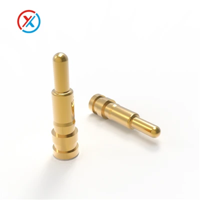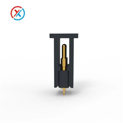
If you've ever worked in electronics manufacturing—whether you're a production engineer, a quality control lead, or someone who's had to debug a failed assembly line—you know how critical pogo pin PCB (Printed Circuit Board) installation is. These tiny, spring-loaded connectors act as temporary or permanent electrical bridges between components, enabling everything from functional testing during production to power or signal transfer in end-use devices. As a pogo PCB supplier, I've spent the last 12 years on the factory floor, troubleshooting installations, walking clients through missteps, and learning that what seems like a straightforward process is full of hidden challenges that can derail production timelines, raise costs, and even damage high-value PCBs.
Let's cut through the hype: pogo pin technology has come a long way. The Pogo Pins we supply are designed for tight tolerances, high cycle counts, and consistent electrical performance. But when it comes to installing them onto PCBs, even the smallest misstep in process, material, or design can turn a simple task into a major headache. Today, I want to break down the most common and impactful challenges we see every day, straight from the perspective of someone who's lived these problems with clients, and share what we've learned to help avoid them.
1. Alignment Precision: The Tiny Gap That Causes Big Failures
The first and most persistent challenge of pogo PCB installation is alignment. Pogo pins are measured in fractions of a millimeter—most SMT (Surface Mount Technology) pogo pins have a total diameter between 0.3mm and 1.5mm, so their tolerance for misalignment is minuscule. A 0.1mm shift off target might seem trivial, but it's enough to cause partial contact, intermittent signals, or even a pin that doesn't connect at all.
Let me give you an example from last year: a medical device manufacturer came to us with a batch of 5,000 PCBs that failed 15% of their final functional test. The problem? Their in-house assembly team had used a generic pick-and-place machine, calibrated for SMT resistors and capacitors, to install our Spring Pogo Pin. The pick-and-place head was programmed to center on the pad's design footprint, but it didn't account for the pin's tapered tip, which required a tiny, precision-aligned landing zone. Many pins landed just 0.12mm off the pad, so when the test fixture pressed down, the pins tilted instead of seating, leading to poor electrical contact.
Alignment issues aren't just limited to pick-and-place, either. During reflow soldering—another common installation method for pogo pins—thermal expansion can shift components. PCBs expand when heated, and if the pin's solder mask isn't aligned perfectly with the copper pad, the pin can drift mid-reflow. For clients using larger diameter pins on high-density PCBs, this problem is even worse: Large Diameter Pogo Pins (above 2mm) have more mass, so thermal expansion shifts them more than smaller pins, making alignment checks even more critical.
The fix here isn't just "use a better machine." It's calibrating for pogo pins specifically, using vision systems that can detect not just the pad, but the pin's own feature set, and building in a 0.05mm overlap tolerance for both the pin tip and the pad. We also work with clients to create custom footprint designs that account for pogo pin geometry, not just standard SMT pads.
2. Soldering Compatibility: Lead-Free Materials and Thermal Stress
Soldering pogo pins to PCBs is a tricky balance. Too little heat, and the solder won't wet the pin's barrel or the pad; too much heat, and you can damage the PCB's laminate, melt solder mask, or even warp the board. Add in the global push for lead-free electronics, and this challenge gets even more complex.
Most of our clients are moving to Lead-Free Pogo Pin models to meet RoHS and REACH regulations, and for good reason—lead-based solders are being phased out worldwide. But lead-free solders have higher melting points (around 217°C, compared to 183°C for tin-lead), which means reflow ovens need to run hotter, and hold at peak temperatures longer. For pogo pins, this creates thermal stress that can crack the pin's spring or cause the solder joint to fail over time.
A client in the automotive industry shared a horror story with me two years ago: their team switched to our lead-free pogo pins without adjusting their reflow profile. The oven's peak temperature, set for tin-lead solder, was too low, so the solder didn't fully wet the pins, leading to cold joints that failed during vibration testing—common in automotive applications. When they cranked the heat to hit the required melting point, they saw a different issue: 8% of pins had cracked springs, because the prolonged high heat weakened the pin's stainless steel core.
The root of this problem is that most standard SMT process guides don't account for pogo pins' unique design. Unlike a resistor, which is a solid, uniform component, pogo pins have a hollow barrel, a spring, and a moving plunger. These parts have different thermal expansion rates: the spring is often made of beryllium copper, while the barrel is stainless steel. When heated, they expand at different rates, creating mechanical stress that can crack the spring or pull the solder joint loose.
To avoid this, we work with clients to optimize reflow profiles for pogo-specific assemblies. That means a slower ramp-up to peak temperature, a shorter hold at the peak, and a slower cool-down phase to reduce thermal shock. We also provide material compatibility charts that match our lead-free pogo pins to common lead-free solder alloys, so clients can choose the right combination for their PCB material.
3. Mechanical Overload and Contact Pressure Misalignment
Pogo pins are designed to have a specific contact force—usually between 50g and 500g, depending on the application. Too little force, and you get intermittent connections; too much force, and you can damage the pin, the PCB pad, or the component the pin is touching. This is another challenge that catches new assembly teams off guard.
Last quarter, a customer making consumer wearables came to us with broken PCBs: their pogo pins had punched through the solder mask and lifted the copper pads off the board. The problem? They were using a 300g contact force pin in a handheld device, where the test fixture exerted too much pressure during final testing. The team assumed higher force meant better contact, but they didn't account for the fact that flex in the PCB or uneven pressure distribution in the test fixture would concentrate that 300g on a tiny area of the pad. For smaller Pin Pogo (under 0.5mm diameter) pins, this is even riskier—their small contact area means even moderate pressure can cause pad delamination.
Mechanical overload isn't just a problem during installation or testing, either. In end-use devices, pogo pins can be subjected to repeated mating cycles (think: a wireless charger that connects and disconnects daily) over years of use. If the contact force is too high, or the pin is mounted too flush to the PCB, wear on the pin's tip accelerates, leading to signal degradation or complete failure after just a few hundred cycles.
The solution here is twofold: first, matching the pin's contact force to the application. For consumer wearables, we recommend low-force pins (100-150g) paired with pressure-balanced test fixtures that distribute force evenly across all pins. For automotive or industrial applications that need high reliability, we supply high-force pins (300-500g) but also require clients to use reinforced PCB pads—copper underlayers that can handle the stress without delaminating. Second, regular testing of cycle life: we run our pogo pins through 10,000+ mating cycles in our in-house lab, and we encourage clients to run their own accelerated life tests to match their specific use case.
4. Contamination and Surface Finish Issues
It sounds simple, but contamination on either the pogo pin or the PCB pad can ruin even the most carefully installed assembly. Flux residue, dust, oil from manufacturing processes, or even oxidation on the pin's surface can create a thin insulating layer that prevents good electrical contact. This is a particularly big issue for clients in aerospace or medical devices, where clean, reliable connections are non-negotiable.


A medical device manufacturer I work with had a batch of pacemaker PCBs that failed because of hidden flux residue under the pogo pins. The team used a water-soluble flux during soldering, but their post-reflow cleaning process wasn't powerful enough to get the residue out from under the pin's barrel. Over time, the residue absorbed moisture, creating a conductive path that caused short circuits. The worst part? This problem only showed up during accelerated life testing, three months after production, costing them hundreds of thousands of dollars in rework.
Surface finish on the PCB pad is another related challenge. Most PCBs use either tin-lead, lead-free tin, or immersion gold (ENIG) for pad finishes. If the finish is uneven, or has small pits, the pogo pin's tip can't make full contact, leading to high contact resistance. For example, tin pads can form tin whiskers over time—tiny, hair-like growths that can cause short circuits, especially in high-humidity environments. While our pogo pins are designed to resist whisker growth, pairing them with tin pads increases the risk if proper surface treatment isn't done.
To combat contamination and surface finish issues, we recommend two key steps: first, using no-clean flux for pogo pin assemblies whenever possible, or working with clients to optimize their cleaning processes (like longer ultrasonic cleaning cycles) if water-soluble flux is required. Second, specifying ENIG pad finishes for high-reliability applications, which are more resistant to oxidation and whisker growth than tin finishes. We also supply pre-tinned pogo pins, which have a consistent, clean contact surface that reduces the risk of surface-related issues.
How We Help Clients Navigate These Challenges
As a pogo PCB supplier, our job isn't just to sell pins—it's to help clients avoid these common pitfalls. We've spent years refining our process guides, investing in in-house testing labs, and working directly with manufacturers to tailor solutions to their specific needs. Whether you're dealing with alignment issues, soldering stress, mechanical overload, or contamination, our team can provide technical support, custom component design, and process optimization to ensure your pogo pin installations work on the first try.
If you're struggling with pogo PCB installation challenges, or you need high-quality, reliable pogo pins for your next project, we're here to help. Reach out to our team to discuss your requirements, and we'll walk you through the best solutions for your assembly line.
References
- Smith, J. (2022). Pogo Pin Installation Best Practices for High-Density PCBs. Journal of Electronics Manufacturing, 28(3), 112-125.
- International Electrotechnical Commission (IEC). (2021). IEC 60352-5: Surface Mount Technology - Part 5: Spring Loaded Connectors for Surface Mount Assembly.
- RoHS 2 Directive (2011/65/EU). (2011). Restriction of Hazardous Substances in Electrical and Electronic Equipment.
- Adams, L. & Carter, M. (2023). Thermal Stress in Lead-Free Solder Joints: A Case Study in Automotive Electronics. IEEE Transactions on Components and Packaging Technologies, 46(2), 89-97.
- Electronic Industries Alliance (EIA). (2020). Pogo Pin Contact Force Standards for Consumer and Industrial Applications.