


Pogo pin connectors can be soldered directly to a PCB, supported in an insulating housing, terminated to wires, or retained between two mating boards. The right mounting method depends on the available space, assembly process, contact force, and loads the finished product will experience.
Two requirements need to be addressed together: establishing the electrical connection and holding the connector in its working position. Solder joints, mounting features, and enclosure supports each have a role. A reliable installation keeps every plunger within its specified working travel while preventing cable pulls, sideways movement, or excessive compression from damaging the contacts.
The following seven arrangements cover different ways to achieve that balance.
Direct surface-mount soldering
A surface-mount pogo pin has a solderable base that sits on a PCB land. Solder paste is deposited, the component is positioned, and a compatible reflow process forms the joint.
This arrangement suits compact layouts and can integrate with automated PCB assembly. It also avoids through-holes and the space needed for protruding tails on the opposite side of the board.
Its reliability depends on the base geometry, land pattern, solder joint, and surrounding mechanical support. Surface mounting is suitable for many applications, but the joint should not be expected to withstand uncontrolled sideways forces. Guides and stops can transfer docking loads into the enclosure while keeping the plunger aligned.
Through-hole soldering with a terminal tail
A through-hole pogo pin has a rear tail that enters a PCB hole and is soldered to the board. The tail helps locate the contact during assembly and provides a different mechanical connection from a surface-mounted base.
This approach is useful where the PCB layout allows holes and access to the soldering side. It requires space for the tail, suitable hole dimensions, and a compatible soldering process.
Inserting a conventional solder tail into a hole does not create a qualified press-fit connection. Solder tails and compliant press-fit terminals require different designs. External support may still be necessary when the connector experiences substantial handling loads.
Surface-mount contacts in an insulating carrier
Multiple pogo pins can be held in a molded insulating carrier and soldered to PCB surface lands. The carrier establishes pin spacing, separates adjacent circuits, and makes the array easier to handle as one component.
Locating pegs help position the housing, while board locks, screws, or other retention features can provide mechanical support where required. A locating peg alone should not be assumed to carry the service loads.
This arrangement is useful for charging docks and compact multi-contact interfaces. The design must control contact coplanarity, housing dimensions, soldering access, and the relationship between the carrier and PCB.
Through-hole contacts combined with a supported carrier
This arrangement combines terminal tails with an insulating carrier. The tails establish the soldered electrical connections, while appropriately designed housing features locate and support the assembly.
It can suit connectors that need controlled pin spacing and substantial mechanical support. The housing may also provide orientation features that reduce assembly mistakes.
The additional features require PCB holes, board area, and a defined assembly sequence. Their positions must agree within the specified tolerances; forcing a misaligned housing onto the board can distort contacts or introduce stress. The benefit comes from a coordinated design, rather than simply adding more attachment points.
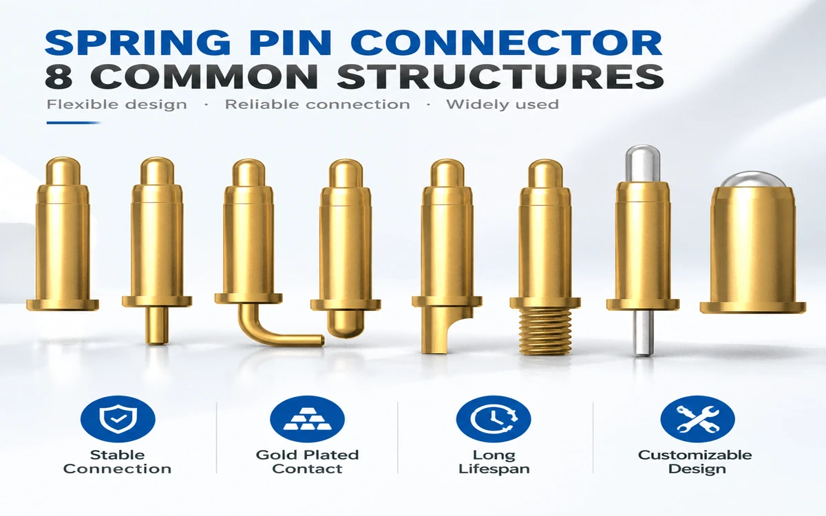
Wire-terminated pogo pins
Wire-terminated contacts allow the pogo pin assembly to be mounted away from the PCB. A solder cup or another purpose-designed termination connects each contact to a conductor, and the wire connects to the board or another connector.
This provides flexibility when the contact face must sit at the enclosure edge, inside a charging cradle, or in a location that the PCB cannot reach directly.
The pogo pins still need secure retention in a carrier or housing. Cable strain relief should transfer pulling and bending loads away from the electrical terminations. Wire size, soldering access, insulation, routing, and allowable voltage drop also influence the finished assembly.
Pogo pins with a rear spring-contact termination
Some designs use a conductive spring tail to contact a PCB pad at the rear of the pogo pin assembly. A carrier or mounting structure holds this tail at its intended deflection while the plunger engages the external mating surface.
This arrangement can accommodate particular side-entry or right-angle layouts and may avoid soldering the rear contact directly to the PCB.
It creates another pressure-contact interface that needs controlled force, suitable plating, and mechanical retention. Board movement must not unload the rear spring. The termination should be engineered for this purpose; bending an ordinary solder tail does not produce an equivalent spring contact.
Double-ended pogo pins between mating surfaces
Double-ended pogo pins provide movable contacts at both ends. They can connect two boards, modules, or contact plates while a carrier retains the pins and the surrounding structure controls the assembly spacing.
This approach can support removable assemblies and accommodate specified variations in board separation. The electrical contact ends do not necessarily require soldering.
Both mating surfaces need suitable pads and alignment. The available travel at each end depends on the internal design, so it should not be assumed that the total compression divides equally between them. Mechanical stops must prevent overcompression, and the assembly must maintain contact at its maximum permitted separation.
The mounting choice becomes clearer once the mechanical loads are defined. A stationary internal board connection has different requirements from a handheld device repeatedly placed into a dock. Cable weight, user handling, vibration, and enclosure movement can all affect the contact position.
For a multi-pin assembly, the supporting structure must accommodate the combined spring force. That force changes with compression, so the design should be checked at both ends of the assembly tolerance range. At minimum compression, every contact must engage adequately. At maximum compression, each pin must remain within its permitted working travel.
Where a standard mounting arrangement conflicts with the device layout, we can develop a coordinated pogo pin or magnetic connector assembly from customer drawings. This can include precision-machined contacts, insulating carriers, mounting features, wire terminations, and mating components. Prototypes or small production batches allow the proposed interface to be checked against the actual PCB and enclosure before larger orders proceed.
PCB dimensions should follow the selected connector's production drawing and recommended footprint. Universal allowances for hole radius, pad size, or tail protrusion can create problems when applied to contacts with different dimensions and soldering requirements.
| PCB feature | What the design needs to establish |
|---|---|
| Through-hole dimensions | Finished hole size, tail dimensions, manufacturing tolerances, and the clearance required by the soldering process |
| Tail protrusion | Board thickness, connector seating position, soldering access, and clearance on the opposite side |
| Surface-mount lands | Contact base geometry, solder-mask openings, paste apertures, and space between adjacent joints |
| Housing locating features | Hole positions, datum references, fit, and whether each feature provides alignment or mechanical retention |
| Mating contact pads | Pin-tip geometry, positional tolerance, permitted movement, and suitable surface finish |
| Component clearances | Space for the housing, assembly tools, inspection, and any required repair access |
A flexible PCB requires additional mechanical consideration. Its thickness alone does not determine the mounting dimensions. A stiffener or enclosure support may be needed to prevent contact force from bending the circuit, reducing compression, or stressing solder joints. The flexing region should also be positioned so normal movement does not concentrate at the connector attachment.
Soldering compatibility must be confirmed for the complete connector. Some pogo pin assemblies are designed for reflow; others are intended for wave, selective, or manual soldering. The approved process must account for the contacts, spring assembly, insulating carrier, and any nearby adhesive or magnet.
Peak temperature, exposure time, and the number of heating cycles all matter. A connector suitable for one production soldering cycle may require a separate assessment before repeated rework. The soldering process should also keep solder and flux from entering the moving contact mechanism.
After assembly, inspection should cover more than the solder joints. Check that the carrier is seated correctly, the contacts remain aligned, and every plunger compresses smoothly and returns freely. Electrical evaluation should use the intended working height and load.
For production approval, representative assemblies should also undergo the required mating, cable-pull, vibration, or environmental tests. Recording the connector revision, PCB footprint, mounting hardware, and soldering process makes those results useful for controlling subsequent production.
1. Which mounting method provides the strongest support?
The answer depends on the load and assembly design. A carrier with dedicated retention features can provide substantial support, but its strength must be assessed together with the PCB and enclosure. Through-hole tails or additional locating pegs alone do not guarantee a stronger finished product.
2. Can all pogo pin connectors withstand reflow soldering?
No. Use a connector specified for the intended reflow profile and number of heating cycles. The insulating carrier and internal assembly must both tolerate the process. Follow the approved soldering conditions for the exact part.
3. Can the same PCB hole and pad allowances be used for every pogo pin?
No. Hole size, land geometry, and tail protrusion depend on the contact dimensions, PCB construction, tolerances, and assembly process. Use the selected connector's drawing and validate the footprint on representative boards.
4. Can pogo pin connectors be mounted without soldering?
Yes. Double-ended contacts, engineered rear spring contacts, and other purpose-designed pressure interfaces can establish connections without soldering the contact ends. They still require secure retention, controlled compression, suitable mating pads, and electrical verification.


