


What Do Pogo Pins Do in a Functional Test Fixture?
Each probe connects an instrument channel to a specific point on the device under test (DUT). The supply, return, and measurement paths serve different purposes.
| Path | Connection through the fixture | Purpose |
|---|---|---|
| Power supply | Supply positive terminal → fixture harness → power probe → DUT input pad | Delivers current to the board |
| Power return | DUT ground pad → ground probe → fixture harness → supply negative terminal | Carries load current back to the source |
| Voltage measurement | Meter sense leads → separate sense probes → DUT output and local ground | Measures the voltage available at the board without including the voltage drop along the load leads |
| Control or feedback | Digital instrument channel → fixture wiring → signal probe → DUT control or status pad | Applies a command or reads the board's response relative to its signal reference |
The same power board can undergo both in-circuit testing (ICT) and functional testing. An ICT continuity check can establish whether the input connector and fuse share an intact electrical path. A functional test powers the board and checks whether its regulator delivers the specified output under load. A board with the wrong feedback resistor could pass the continuity check and still produce the wrong voltage.
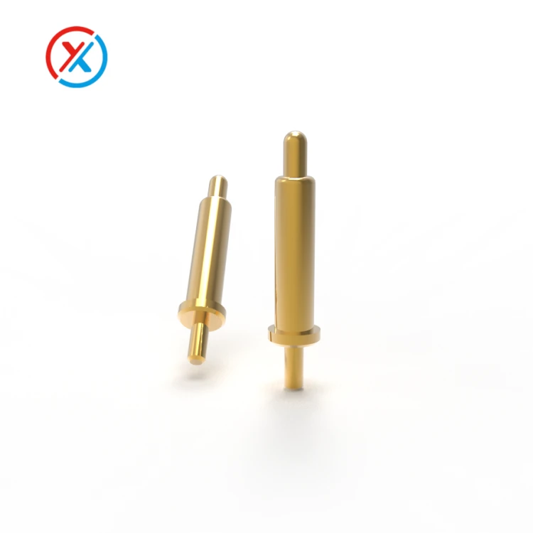
Inside a typical test probe, the plunger carries the tip that touches the board. The barrel guides its movement, and the spring supplies contact force as the fixture closes. A receptacle, when used, holds the probe in the fixture and allows individual replacement. The fixture's closed position sets the working stroke. Too little compression can leave a marginal contact. Too much can damage the probe or bend the board.
Which Functional Tests Can Use Pogo Pins?
| Test task | Probe access points | What the test system checks |
|---|---|---|
| Power-up and current consumption | Supply, ground, and enable | Whether the board starts in the required time and draws the expected standby and operating current |
| Input and output response | Control input, output, status, and reference ground | Whether a defined input produces the expected output and feedback under the specified load |
| Communications | Data lines and a nearby signal reference | Whether the device recognizes a command and returns the correct data within the allowed time |
| Functional verification after programming | Programming interface, reset, and communications port | Whether the device restarts, reports the expected firmware version, and completes a command that exercises the programmed function |
For firmware verification, reading back a version number is a useful identity check. Asking the board to switch an output and then measuring that output also exercises the path from software to hardware. Choose the command according to the fault the test needs to detect.
How Do You Select the Right Test Probe?
Match the tip to the test point
Start with the surface the tip will actually touch. A smooth, flat pad that must remain suitable for a customer-facing contact may call for a rounded tip and a limit on the permitted witness mark. A plated through-hole can take a tip designed to make contact at its rim. A protruding component lead may suit a cup-shaped tip that keeps the lead centered. Check the tip against the smallest target and the largest expected positioning error. A mark near the edge of a pad can reveal a problem that a continuity reading misses.
Set working stroke and calculate total force
Use the probe's force at the intended compression. For example, INGUN specifies 1.5 N at a recommended working stroke of 4.3 mm for its S-031-0005 via probe. Its maximum stroke is 6.35 mm. If a fixture uses 40 of those probes at the recommended stroke, their calculated combined spring force is 60 N. That figure excludes other forces the closing mechanism must overcome.
Check where that force acts. A cluster of probes beneath one corner can bow an unsupported board even when the clamp can supply the total force. Board thickness, support height, and probe installation depth all affect the actual compression.
Select power and signal probes for different duties
For a power connection, measure the voltage at the DUT while the intended load flows. Check both the supply and return paths for voltage drop and temperature rise. For a communications link, pay attention to the probe, its return path, and the wiring between the fixture and instrument. Verify the link at the intended data rate. A successful low-speed command can conceal a fixture problem that appears at production speed.
On a frequently used station, consider how a technician will replace a damaged tip. A receptacle-mounted probe can often be exchanged without disturbing the harness. For a fine-pitch fixture, also compare socketless options and check how much access the replacement tool needs once the probe plate is installed.
How Should the PCB and Test Fixture Be Designed Together?
Choose test points while the PCB layout can still change. Identify the accessible side, exposed target diameter, center-to-center spacing, and clearance to surrounding components. A pad can look accessible in the PCB file while a tall component prevents the fixture from closing. On the fixture drawing, show the board location features, direction of closure, probe travel, and supports beneath areas of concentrated force.
Maintain a channel map that includes the instrument terminal, fixture probe number, PCB net, and test purpose. For example, an entry might read DMM channel 2 positive → fixture P07 → VOUT_SENSE → loaded output voltage, with a separate entry for its local ground reference. If a station reports a low output, that record tells the technician exactly which two points produced the reading.
For fine-pitch or double-sided fixtures, send the PCB test-point drawing and a section view of the closed fixture to Dongguan Xinteng Electronics Co., Ltd. for a drawing-based pogo pin assessment. Include the access direction, available stroke, and component keep-out areas on each side. These details help establish whether a standard probe will fit or whether the probe plate, board supports, or locating features need a different arrangement.
How Can You Tell a Product Failure from a Contact Problem?
| What happens on the station | What to inspect first | How to distinguish the causes |
|---|---|---|
| The same board passes after the fixture is reopened and closed | Sticking plunger, off-center landing, residue, or a loose board locator | Inspect the witness marks and cycle a known-good board through the same station. Retain the first failure record. |
| Board voltage falls below its limit under load | Power and return probes, harness, terminations, and source current limit | Measure voltage at the source terminals and DUT pads under the same load. Measure the drop on each conductor separately. |
| A communications test occasionally times out | Signal contact, reference ground, fixture routing, reset timing, and DUT response | Cross-check the board on a second station. Capture the command and response at the DUT if the timeout persists. |
| Several boards fail at the same fixture position | Probe, receptacle, wire termination, or channel assignment | Run a known-good board, check the channel map, then replace or repair one suspect part at a time and repeat the test. |
A retest pass gives a reason to investigate. It does not identify the fault. Reclosing the fixture can restore a weak probe contact, but pressure can also temporarily close a cracked solder joint on the board. Checking whether the failure follows the board, the station, or a particular probe position is more informative than repeatedly testing until the unit passes.
Worked Example: Functional Testing of a Charging Board
Texas Instruments documents a load-step test for its bq25570 energy-harvesting battery charger evaluation module in user guide SLUUAA7A, Revision A. The board combines a charger with a regulated buck output. Its published schematic, test-point labels, and oscilloscope record make it possible to trace a real measurement from the applied load to the board's response.
| Test detail | TI's published setup or record |
|---|---|
| Input | A 2.0 V source feeds VIN_DC through 100 Ω. The series resistance is part of the test setup. |
| Storage element | A rechargeable 4.2 V coin cell at 3.2 V connects to VBAT. |
| Output load | A switch connects 36 Ω to VOUT. At the nominal 1.8 V output, that gives a 50 mA load step. |
| Measurement points | TP1 measures VIN_DC, TP4 measures VSTOR, and TP6 measures VOUT, each relative to board ground. A current probe measures output current. |
| Recorded response | Figure 8 shows the measured output-current step alongside VIN_DC, VSTOR, and VOUT. The traces show when the load was applied and how the output and storage node responded. |
The distinction between a specified limit and a recorded waveform matters here. TI lists a buck output set-point range of 1.75 to 1.85 V for output current below 95 mA, with ripple and line and load regulation excluded. Applying that range to every instant of the 50 mA load step would misread the specification. A production test needs separate, approved limits for the settled output, allowable transient excursion, and recovery time.
A pogo-pin fixture can adapt the documented bench test as follows:
Locate and support the board with the fixture sources disabled. Close the fixture and verify contact at the designated pads.
Establish the input and storage conditions. Measure VIN_DC at TP1 so the record shows the voltage reaching the board.
Apply the switched load. Capture output current and TP6 voltage together, using a local ground reference. TP4 helps show what happened at the storage node during the same event.
In a separate status check, move the storage voltage through the board's defined battery-good thresholds and read VBAT_OK. Record the state change in each direction.
Remove the load, disable and isolate the fixture sources, then release the board.
Figure 8 is TI's bench measurement. The pogo-pin sequence is a proposed fixture implementation. For a production run, the corresponding record should identify the DUT, fixture and program revisions, probe positions, applied load, measured values, and limits used for the decision.
How Do You Keep Pogo Pin Test Results Repeatable?
Before releasing the fixture, load and unload a known-good board several times and compare the actual readings. Watch the channels closest to their limits. A string of passes can hide a voltage reading that moves each time the fixture closes. Then run a board with a documented fault and confirm that the intended test step detects it. For a charger, a known status-output fault can check whether the program really reads the feedback line.
During production, track first-pass yield and retest results separately by station, test step, and probe position. If several products begin failing on one station's ground return, inspect that path before changing the product limits. Keep the probe part number, fixture revision, maintenance date, and readings from before and after cleaning or replacement. Those records let the next technician see what changed and whether the repair restored repeatability.
Technical References
Texas Instruments. User's Guide for bq25570 Battery Charger Evaluation Module for Energy Harvesting. Document SLUUAA7A, revised August 2014. Sections 1.4, 2, and 3.1.3, Figures 7 and 8.
INGUN Prüfmittelbau GmbH. Test Probe S-031 238 040 A 1500 S. Product datasheet, item S-031-0005, edition 12/25_GB.


