


Basic Terms: Test Object, Inspection Method, and Acceptance Criteria
| Term | Meaning | Example in a report |
|---|---|---|
| Printed circuit board (PCB) | The board carrying the conductive traces, pads, and vias. "Bare PCB" identifies an unpopulated board. | Bare PCB, fabrication revision C |
| Printed circuit board assembly (PCBA) | A board with components mounted and electrically connected. The assembly can have its own revision. | Charging PCBA revision D, built on bare PCB revision C |
| Device under test (DUT) | The item connected to the test system. It may be a component, board, or complete device. | DUT serial number 0042 |
| Unit under test (UUT) | The unit evaluated by a test procedure. Production software may call the same assembled board a UUT. | UUT 0042, fixture F02 |
| Inspection | Examination of a physical feature against defined criteria. | An optical image shows solder between two adjacent leads on U3. |
| Test | A measurement or applied stimulus used to evaluate a characteristic or response. | Resistance measured between U3 pins 4 and 5. |
| Acceptance criteria | The documented conditions that determine whether a result passes. | Evaluate the solder connection against the specified workmanship clause and product class. |
Consider the solder between the two leads on U3. The image records what the inspector saw. The resistance reading shows whether an electrical path exists. The schematic establishes whether the leads are intended to connect, and the applicable workmanship criterion determines whether the physical condition is acceptable. Keeping those findings separate prevents an observation from becoming an unsupported diagnosis.
Bare-Board Testing: Continuity, Isolation, Opens, and Shorts
A net is a set of points intended to share an electrical connection. A netlist identifies those points. Suppose the design assigns connector pad J1-1 and test point TP3 to the input supply, VIN, and assigns TP4 to ground. The tester can check continuity between J1-1 and TP3, then check isolation between VIN and ground. Record the netlist revision alongside the board revision. A tester running an obsolete netlist can correctly execute the wrong checks.
| Term | What the test examines | Evidence to check |
|---|---|---|
| Continuity | Whether intended connections meet the specified resistance limit | Net name, endpoints, resistance limit, and result |
| Open circuit | A break in an intended path. A tester can also report an "open" when resistance exceeds its programmed threshold. | Failed endpoints and an independent reading taken directly at the pads |
| Isolation test | Whether nets intended to remain separate meet the specified minimum resistance | Net pair, applied test voltage, resistance threshold, and result |
| Short circuit | An unintended low-resistance connection between conductors | Affected nets, measured resistance, and confirmed location where available |
An open indication has several possible explanations. A trace may be broken, a via may have excessive resistance, or a probe may have landed on residue. A direct measurement at the same pads helps separate a board fault from a fixture contact problem. Likewise, a failed isolation test warrants a resistance measurement before the report identifies a metallic short. Surface contamination can also create a leakage path.
Flying-probe testing uses movable probes to contact programmed locations in sequence. A bed-of-nails fixture uses an array of probes positioned for a particular board layout. Either report should identify the board, the tests performed, and any inaccessible or excluded nets. The equipment name alone cannot establish coverage.
Assembly Inspection and Testing: SPI, AOI, AXI, ICT, and FCT
| Method | What it checks | What to look for in the report |
|---|---|---|
| Solder paste inspection (SPI) | Paste deposits after stencil printing | Pad identifier and the measured height, area, volume, or offset that triggered the result |
| Automated optical inspection (AOI) | Optically visible features, including component presence, placement, polarity marks, and exposed solder joints | Flagged image, inspection program revision, and the reviewer's decision |
| Automated X-ray inspection (AXI) | Internal features visible in an X-ray image, including hidden solder joints | Component and joint location, image view, observed feature, and applicable criterion |
| In-circuit test (ICT) | Connections and selected component characteristics measured through accessible circuit nodes | Component reference, nodes accessed, test limits, measured values, and exclusions |
| Functional test (FT or FCT) | The powered assembly's response to a defined input, command, or load | Board input, load, firmware and program versions, measurement points, and output limits |
In in-circuit test, the component remains connected to the surrounding circuit. For example, a resistor measured through two test points may have another conductive path in parallel. The ICT program must account for that path when setting its limits.
On the same charging board, AOI might inspect regulator orientation, ICT might check a feedback resistor, and FCT might measure the regulated output at a 1 A load. Each result supports a different conclusion. Use the project's abbreviation list when reading reports, particularly where two factories use different names for the same functional test step.
Test Fixture and Probe Terminology
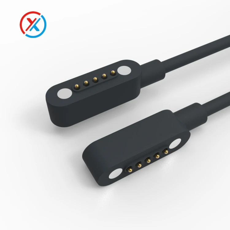
A test point is a designated location on the board. A test probe makes temporary electrical contact with it. In a spring-loaded probe, commonly called a pogo pin, the tip retracts as the fixture closes. A receptacle holds a replaceable probe and connects it to the fixture wiring. The test fixture locates and supports the board while making those connections.
Probe numbers and PCB test-point numbers belong to different drawings. A channel map connects them:
| Instrument connection | Fixture wire | Fixture probe | Board test point | Purpose |
|---|---|---|---|---|
| Voltmeter positive input | W12 | P07 | TP6, VOUT | Sense output voltage at the board |
| Voltmeter negative input | W13 | P08 | TP7, local ground | Establish the reference for that reading |
Pitch is the center-to-center spacing between probe positions. Working travel, or working stroke, is the distance the plunger moves from its unloaded position when the fixture closes. Contact force is the force applied at a stated compression. A force value becomes useful only when the report gives the stroke or installed height at which it was measured.
For a fixture contact review, Dongguan Xinteng Electronics Co., Ltd. can use the board's test-point drawing, pad finish, probe pitch, and closed fixture height to assess a pogo pin against the intended application. Including the instrument channel map helps distinguish a contact that carries load current from one used to sense voltage.
Contact Resistance and Four-Wire Measurement
Contact resistance is meaningful only when the measurement endpoints are identified. A reading from a probe terminal to a PCB pad includes the probe's internal conductive path and its contact with the pad. Moving one endpoint back to the fixture connector adds wiring and terminations to the reading.
In a four-wire, or Kelvin, measurement, one pair of leads supplies the test current and a separate pair senses voltage at the chosen endpoints. Resistance is calculated from the sensed voltage divided by the applied current. Mark both sense points on the fixture drawing. That allows a technician to repeat the original measurement after replacing a probe or repairing a wire.
Reading Results: Limits, Coverage, False Failures, and Escapes
Nominal Value, Tolerance, and Test Limits
The nominal value is the design target. The tolerance defines the permitted variation. The lower and upper limits give the acceptance interval, and the measured value records what the instrument read.
For example, suppose a product specification calls for 5.00 V ±5% at the board's output pads under a 1.00 A load. The permitted range is 4.75 to 5.25 V. A reading of 4.70 V fails by 0.05 V. Recording the value and its units preserves information that a single "Fail" entry would lose.
Node, Fault, and Functional Coverage
| Coverage term | Question it answers | What the percentage must identify |
|---|---|---|
| Node coverage | Which defined circuit nodes did the tester access or test? | Total nodes in scope, inaccessible nodes, and whether the count represents physical access or an executed test |
| Fault coverage | Which faults in a defined set can the test detect? | Fault model, exclusions, and whether detection was predicted or verified using known faults |
| Functional coverage | Which required product functions did the program exercise? | Approved function list, tested operating modes, loads, and excluded features |
If a board has 100 design nets and the program tests all 90 accessible nets, the result is 100% of accessible nets or 90% of design nets. The denominator determines what the claim means.
False Fail, Test Escape, and First Pass Yield
A false fail occurs when a conforming unit receives a failure result. A sticking probe can cause a good charging board to fail under load. Passing after the fixture is reopened is a reason to investigate. Confirm the diagnosis by checking the affected path and testing the board on an independently verified station.
A test escape occurs when a defective unit passes through the applicable test without detection. A program might read the expected firmware version yet omit the command that enables charging. A board with a defective output switch could then pass. Running a sample with that confirmed fault shows whether the revised program detects it.
First pass yield (FPY) counts units that pass on their first attempt. If 100 boards enter FCT, 92 pass immediately, five pass on retest without repair, and three pass after repair, FPY is 92%. All 100 may eventually pass, but the first failures still matter: they reveal how often the process required a second test or a repair.
Which Standard Governs the Result?
| Document | Where it applies | What to verify |
|---|---|---|
| IPC-A-600, Acceptability of Printed Boards | Bare-board acceptability, read with the applicable performance and procurement requirements | Specified revision, product class, board feature, and clause |
| IPC-9252, Requirements for Electrical Testing of Unpopulated Printed Boards | Bare-board electrical test data, methods, parameters, and fixtures | Invoked revision, test level where applicable, netlist revision, limits, and exclusions |
| IPC-A-610, Acceptability of Electronic Assemblies | Workmanship and acceptance criteria for electronic assemblies | Specified revision, product class, joint or component type, and clause |
| J-STD-001, Requirements for Soldered Electrical and Electronic Assemblies | Materials, processes, and acceptance requirements for soldered assemblies | Specified revision, applicable class and addenda, and process or feature under review |
| Project drawing, procurement specification, and test procedure | Product-specific dimensions, electrical limits, functional requirements, and sampling | Document number, revision, test-step identifier, and agreed order of precedence |
Use the revision identified in the purchase agreement or approved quality plan. IPC lists IPC-9252B as no longer maintained, although a project may still invoke that revision. For an assembly example, IPC-A-610J clause 8.3.12.4 addresses voids in surface-mount area-array solder connections. The allowable output voltage of a particular charging board comes from its approved product or functional test specification.
Worked Example: Tracing a Low Output Voltage Failure
The following teaching example follows one charging interface board through an initial failure, diagnosis, and retest. Its identifiers and readings are illustrative.
| Unit and test identity | Test condition | Measurement points | Accepted range | First result |
|---|---|---|---|---|
| PCBA rev D, unit 0042, firmware 1.3, fixture F02 rev C, program 2.4 | Step FCT-07, 5.10 V source setting, 1.00 A output load | TP6 VOUT to TP7 local ground | 4.75–5.25 V | 4.70 V, Fail |
Confirm the observation. This board routes its 5 V input through a controlled output switch. The first run establishes that the loaded output at TP6 was low. It leaves the cause open.
Measure the input at the board. An independent meter reads 5.10 V at the source terminals and 4.74 V at the board input pads under the same load. The incoming supply and return paths together drop 0.36 V. Only 0.04 V separates the board's input and output readings. Those measurements direct the investigation toward the fixture before anyone replaces the output switch.
Check whether the fault follows the board or the station. A known-good board also shows a low input on F02. Unit 0042 passes on a verified second station. Back on F02, a measurement from the supply probe terminal to its mating pad shows 0.32 V across that section under load. Most of the incoming loss is now localized to the probe path and its interface with the board.
Preserve both results. After replacing the suspect probe, the technician repeats the test with the known-good board and then measures 5.04 V on unit 0042 at TP6–TP7. The unit record retains the 4.70 V first failure, diagnostic readings, probe position, maintenance action, and linked retest. A buyer reviewing the batch can see why the board was released and why its first run still counts as a failure in FPY.
Abbreviation Index
| Abbreviation | Full term | Abbreviation | Full term |
|---|---|---|---|
| AOI | Automated optical inspection | ICT | In-circuit test |
| AXI | Automated X-ray inspection | PCB | Printed circuit board |
| DUT | Device under test | PCBA | Printed circuit board assembly |
| FCT / FT | Functional test | SPI | Solder paste inspection |
| FPY | First pass yield | TP | Test point |
| GND | Ground | UUT | Unit under test |
| VIN | Input voltage | VOUT | Output voltage |
Technical References
IPC. IPC-9252B: Requirements for Electrical Testing of Unpopulated Printed Boards. September 2016. Sections 1 and 1.1, scope and purpose.
IPC. IPC-A-610J: Acceptability of Electronic Assemblies. March 2024. Section 1.1, scope, and Section 8.3.12, surface-mount area arrays.


