


Gold plating, a small diameter, or a short signal path can contribute to a suitable design. None establishes a data-rate rating on its own.
For hardware engineers and procurement teams, the objective is to select a contact assembly supported by relevant electrical data, then verify it within the intended product.
The first distinction is between per-lane signaling rate and aggregate bandwidth. Adding lanes increases total throughput without necessarily increasing the signaling frequency on each lane.
For NRZ signaling, the Nyquist frequency is half the symbol rate. For PAM4, two bits are represented by each symbol, so the Nyquist frequency is one-quarter of the raw bit rate.
| Interface or signaling example | Physical signaling rate | Modulation | Nyquist frequency |
|---|---|---|---|
| USB 3.0 / USB 3.2 Gen 1 | 5 Gb/s per lane | NRZ | 2.5 GHz |
| USB 3.2 Gen 2 | 10 Gb/s per lane | NRZ | 5 GHz |
| USB 3.2 Gen 2×2 | Two 10 Gb/s lanes, providing 20 Gb/s aggregate | NRZ | 5 GHz per lane |
| PCIe 4.0 | 16 GT/s per lane | NRZ | 8 GHz |
| PCIe 5.0 | 32 GT/s per lane | NRZ | 16 GHz |
| Nominal 112 Gb/s PAM4 example | 56 GBd per lane | PAM4 | 28 GHz |
| Nominal 224 Gb/s PAM4 example | 112 GBd per lane | PAM4 | 56 GHz |
The USB and PCIe entries describe physical signaling rather than application payload throughput. USB 3.2 Gen 2×2 reaches 20 Gb/s by combining two 10 Gb/s lanes; treating it as a single 20 Gb/s NRZ lane would produce the wrong frequency calculation.
For final calculations, use the actual line rate specified by the interface. Labels such as "112G" and "224G" can describe a performance class rather than the exact encoded bit rate of every implementation.
Nyquist frequency is a useful reference, but it is not the upper limit of all relevant signal content or a sufficient connector qualification boundary. Channel response beyond Nyquist, resonances, noise, and receiver equalization also affect signal recovery.
Even at 5 Gb/s, the pogo pin interface needs more than low contact resistance. Differential-pair geometry, ground continuity, mating pads, cable construction, and PCB launches can determine whether the link operates reliably.
As the signaling rate increases, these details require closer analysis. The appropriate design may use a shorter compression interface, dedicated ground contacts, shielding, or revised PCB routing. The choice should follow the channel requirements rather than a rule that assigns one contact construction to every speed category.
Four electrical characteristics deserve particular attention.
| Characteristic | What to evaluate | Why it matters |
|---|---|---|
| Insertion loss | Transmission magnitude and phase across the required frequency range | Excessive or uneven attenuation reduces the signal available to the receiver |
| Impedance and return loss | Impedance discontinuities, reflections, and resonances | Mismatches can distort the received waveform |
| Crosstalk | Coupling from neighboring active channels | Aggressor signals can reduce the available noise margin |
| Mode conversion | Conversion between differential and common-mode signals | Pair imbalance can affect signal quality and electromagnetic behavior |
These measurements must describe the intended configuration. A single contact tested with generous spacing may behave differently in a dense array. Ground allocation, neighboring signals, carrier materials, and the mating PCB all contribute to the result.
Loss terminology should also be consistent. If the design permits no more than 0.5 dB of connector insertion loss, the insertion-loss magnitude is ≤0.5 dB. Expressed as differential transmission magnitude in decibels, the corresponding requirement is SDD21 ≥−0.5 dB.
Likewise, return loss of ≥15 dB corresponds to a reflection magnitude of SDD11 ≤−15 dB. These are examples of specification notation, not universal limits for every high-speed connector.
The impedance target must come from the intended interface. An 85-ohm reference used for one socket does not establish the requirement for every PAM4, USB, or Ethernet connection. The report should identify the reference impedance and how the connector's measurement boundaries relate to the complete channel.
An eye diagram needs context as well. Transmitter settings, receiver equalization, test pattern, measurement location, and the surrounding channel all affect its appearance. Error-rate evaluation should define the operating conditions and, where relevant, whether results are measured before or after error correction.
A connector supplier may provide component models and samples while the OEM or test laboratory owns complete-link validation. Those responsibilities should be agreed before development begins.
Five integration problems are particularly useful to address during selection.
The bench assembly differs from the finished product
A favorable laboratory result may use different PCB launches, cables, compression, or grounding from the production assembly. These differences can explain a loss of margin after installation.
Evaluate representative hardware across the permitted compression and temperature ranges. Where vibration or movement is part of normal use, monitor link errors and interruptions under those conditions. Static continuity alone cannot establish high-speed performance.
The supplied data do not match the proposed part
A simulation or test report is useful only when its geometry and conditions are identifiable. A result from a different pin height, carrier, plating revision, or ground arrangement may not apply to the selected assembly.
Request the relevant model or S-parameter files, drawing revision, operating position, and fixture description. Keep design targets, simulations, prototype measurements, and qualification results clearly distinguished.
Pitch is reduced without revisiting the return paths
Moving contacts closer together changes their electromagnetic coupling. Preserving the same signal assignment while removing ground positions can affect impedance and crosstalk.
Review the complete array, including neighboring aggressor channels and ground connections into the PCB. A metal barrel carrying the signal is not automatically a grounded shield. Any shielding feature needs an intentional, electrically continuous connection to its reference.
Power and data are validated separately
A connector may pass a signal test at light load but behave differently when nearby power contacts heat the assembly. Switching currents can also introduce noise through shared return paths or coupling.
Test data transmission while the intended power circuits operate. Review conductor resistance, terminations, current sharing, thermal paths, and return-current routing. There is no universal current-and-frequency threshold that defines when these interactions become significant.
Tolerances are specified without a functional inspection plan
Barrel geometry, plunger alignment, plating buildup, and assembly distortion can affect movement and contact consistency. The importance of a dimensional variation depends on the design; a single tolerance value cannot serve as a universal high-speed requirement.
Identify the critical finished dimensions and select inspection methods that can measure them. Optical inspection, dimensional metrology, sectioning, or X-ray may each have a role. Their suitability depends on the feature and defect being investigated.
Mechanical requirements remain important throughout this process. The contact should provide the required force across the assembled tolerance range while retaining enough travel to avoid overcompression. The housing or mounting structure should control lateral movement and carry the intended mechanical loads.
Contact force also needs to be considered across the whole array. Increasing force can change friction, wear, board loading, and retention requirements. It should not be used as a general remedy for an unsuitable conductive path.
Materials and plating should be selected for their actual function. The mating finish needs suitable wear and corrosion performance, while the base material and internal interfaces influence conduction and mechanical behavior. Plating thickness must be controlled at the specified locations and included in the finished dimensional requirements.
For custom products, we can work from customer drawings to develop pogo pin or magnetic connector assemblies around the available space and electrical architecture. This can include precision-machined contacts, insulating carriers, mating components, mounting features, and cable terminations. Samples or small batches allow mechanical fit and functional performance to be assessed before the design is released for production.
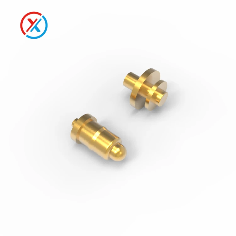
A high-speed development brief should define:
The interface, lane count, actual signaling rate, and required channel performance.
Contact assignments, grounding, shielding, and mating orientation.
Installed height, working compression, contact force, and dimensional tolerances.
Continuous and peak power requirements, including simultaneous power-and-data operation.
Relevant models, fixture design, measurement boundaries, and acceptance criteria.
Environmental exposure, expected mating cycles, and production inspection requirements.
Electromagnetic simulation can help compare proposed geometries and locate coupling or resonance problems. Its value depends on representative materials, geometry, boundaries, and correlation with measurements. The name of the software does not establish the quality of the analysis.
Production approval should remain linked to the tested configuration. Changes to pin height, carrier material, plating, ground assignment, or termination can require an appropriate review. The approved drawing, electrical model, inspection plan, and qualification results should describe the same assembly.
1. Is a standard gold-plated pogo pin sufficient for USB 3.0?
Gold plating can support a stable contact surface, but it does not establish 5 Gb/s capability. The contact arrangement, differential pairs, return paths, mating pads, and PCB or cable transitions must meet the intended USB channel requirements.
2. Does USB 3.2 Gen 2×2 require a 10 GHz Nyquist frequency?
No. It combines two 10 Gb/s NRZ lanes, giving a Nyquist frequency of 5 GHz per lane. Connector evaluation still needs to cover the frequency range and performance criteria required by the complete interface.
3. Does a connector tested to 90 GHz automatically support 224G PAM4?
No. The report must explain what was measured and whether the relevant loss, reflection, crosstalk, and mode-conversion requirements were met. The assembled channel also needs validation under its intended operating conditions.
4. What should an OEM request before ordering a custom high-speed pogo pin connector?
Request a controlled drawing, applicable electrical models or measurements, mechanical operating limits, and a defined sample-validation plan. Agree who will verify the complete channel, simultaneous power loading, durability, and production consistency.


