


Their specification needs to cover more than size. Barrel diameter, installed height, working travel, contact force, and electrical performance together determine whether a miniature contact will suit the device. High-speed capability requires particular attention to the complete signal path.
For products with unusual space constraints, we can develop miniature pogo pin or magnetic connector assemblies from customer drawings. This can include precision-machined plungers and barrels, insulating carriers, mating components, and terminations. Reviewing these parts together helps resolve contact positioning and assembly issues before samples are produced.
The term "micro" describes a small contact format, but it does not provide a complete dimensional specification. If a project requires an outside diameter below 0.8 mm, the drawing should identify the relevant feature, its tolerance, and whether the dimension applies before or after plating. Pitch, housing width, and working height need separate definitions.
A small barrel diameter can support a compact arrangement, although the finished connector also needs space for insulation, contact retention, PCB routing, and mechanical guidance.
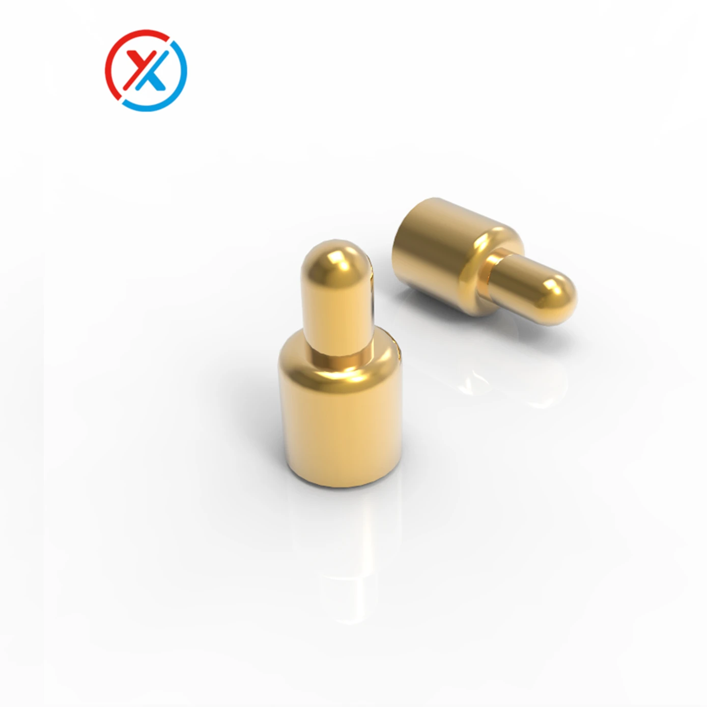
The basic construction remains familiar: a movable plunger sits inside a barrel and is supported by a spring. When the mating surface presses against the tip, the plunger moves inward and the spring develops contact force. The internal conductive path depends on the contact design, including how the plunger engages the barrel.
Miniaturization makes the relationships between these parts more demanding. A burr, plating buildup, or small dimensional variation can consume a significant proportion of the intended running clearance. A contact that moves freely before plating may bind afterward if the finished dimensions have not been considered.
Precision turning, spring forming, surface preparation, plating, and assembly therefore need coordinated control. Inspection should address bore condition, plunger alignment, retained travel, and smooth return as well as external dimensions. A machine's stated resolution alone does not establish the accuracy or consistency of the finished contact.
For thin devices, working travel is often as important as diameter. The contact must remain compressed sufficiently at the largest assembled gap while avoiding excessive compression at the smallest gap. PCB position, housing dimensions, mating-pad height, and assembly tolerances all contribute to that range.
Mechanical stops should establish the final seated position. The plungers should not carry loads that belong in the enclosure or mounting structure. Their spring travel accommodates specified axial variation; guides are still needed to control sideways displacement and angular misalignment.
Contact force also becomes a system-level consideration in a dense array. A modest force from each pin can produce a substantial combined load when many contacts engage simultaneously. The PCB, carrier, fastening arrangement, and mating surface must maintain their position under that load without excessive bending.
Electrical performance introduces a separate set of requirements. Low contact resistance helps control voltage drop and resistive heating, but it does not establish high-frequency performance. At higher frequencies, the geometry of the conductive path and its surroundings affects impedance, reflections, and coupling between signals.
A shorter contact may help reduce some parasitic effects, while a smaller pitch can increase interaction between adjacent conductors. The result depends on the signal and ground arrangement, mating pads, PCB transitions, housing materials, and working compression.
For differential signals, both conductors need an appropriate relationship to each other and to their return paths. For radio-frequency interfaces, the contact structure and shielding arrangement must suit the intended impedance and frequency range. A generic miniature pin should not be assigned a bandwidth based on diameter alone.
Useful validation may include insertion loss, return loss, crosstalk, and time-domain impedance measurements. Eye-diagram or error-rate testing can then assess the intended digital interface in a representative assembly. Test reports should identify the contact arrangement, compression, PCB construction, and measurement boundaries so the results can be applied correctly.
Power capability must also be evaluated independently. Reducing the conductive cross-section can increase resistance and limit heat dissipation. Current capacity depends on the plunger, barrel, internal interfaces, mating pads, and terminations under the specified operating conditions.
In a dense array, adjacent power contacts can influence each other's temperature. Parallel contacts may also share current unevenly. Thermal testing should therefore use the intended contact assignments and loading pattern rather than simply adding individual pin ratings.
Materials and plating need to support both the mechanical and electrical requirements. Copper alloys can provide suitable conductivity and machinability for contact bodies, while spring material selection depends on force, dimensions, temperature, and fatigue requirements. The spring's electrical contribution varies with the internal design.
A gold finish over an appropriate underlayer is one option for maintaining a stable contact surface. Its effectiveness depends on coverage, thickness, adhesion, wear, and the opposing material. Specifying these characteristics at functional locations is more useful than describing the part only as "gold plated."
Miniature spring contacts can serve several application types, each with different priorities.
| Application | Possible role for micro pogo pins | Main engineering considerations |
|---|---|---|
| Semiconductor test sockets | Temporary electrical access to package terminals or test pads | Pitch, tip geometry, contact force, signal path, cleaning, and replacement |
| Compact board-to-board interfaces | Removable power or signal connections between closely spaced assemblies | Installed height, board support, alignment, total compression force, and routing |
| Portable electronics and wearables | Charging, identification, service, or accessory contacts | Available space, repeated mating, contamination, and environmental exposure |
| Sensor and instrument modules | Connections for removable sensing or measurement assemblies | Resistance stability, signal requirements, mounting repeatability, and maintenance |
| Robotic modules and docking interfaces | Connections for sensors, accessories, or specified charging functions | Retention, vibration, cable loads, contact wear, and electrical demand |
Semiconductor testing and permanent equipment interconnects require different evaluations. A miniature probe used to test a processor does not establish that the same design is suitable for a permanent GPU socket or server backplane. Processor and optical-module projects need evidence for their particular electrical interface, mechanical arrangement, and operating conditions.
The same distinction matters in robotics. A compact contact used for a sensor or battery-identification signal may have very different requirements from a main battery power connection. Movement tolerance, current capacity, and environmental protection should be assessed for the assigned function.
Prototype evaluation should use the intended carrier, mating surfaces, and mounting arrangement wherever possible. Alongside electrical measurements, check plunger movement, force at the working position, and the assembled tolerance range. Durability testing should define both the number of cycles and the acceptable changes in resistance, force, and surface condition.
For drawing-based production, critical dimensions and inspection criteria should remain linked to the approved sample configuration. Changes to plating, spring geometry, carrier material, or mounting height can affect performance even when the connector looks unchanged.
1. Must a micro pogo pin have a diameter below 0.8 mm?
The term alone is insufficient as a dimensional requirement. If a project specifies a diameter below 0.8 mm, identify the relevant feature, tolerance, and finished condition on the drawing. Pitch, working height, and travel must also be specified.
2. Can micro pogo pins support high-speed data transmission?
They can be incorporated into designs developed for high-speed signals. Capability depends on the contact arrangement, return paths, PCB transitions, and complete interface. Confirm performance through measurements appropriate to the intended protocol and data rate.
3. Are micro pogo pins suitable for high-current battery connections?
Suitability depends on the specific contact and assembled power path. Check resistance, voltage drop, temperature rise, and continuous or peak-current conditions. A contact suitable for battery sensing or identification is not automatically suitable for the main power circuit.
4. What information is needed to customize a micro pogo pin assembly?
Provide the mechanical drawings, contact layout, available space, assembled gap, and mounting method. Electrical requirements, target contact force, mating frequency, and environmental conditions help define the contact geometry, materials, plating, and sample-validation plan.


